UNIST site map
- Admissions
-
Academics
- Colleges and Schools
-
Academic Affairs
- Academic Calendar
- Academic Curriculum
- Requirements for Graduation
- Browse Open Courses
- Undergraduate Administration
-
Graduate Academic Affairs
- Tuition Fee Payment
- Academic Leave of Absence/ Academic Return
- Voluntary Withdrawal/ Expulsion
- Change of Major
- Change of Degree Program/ Dropping of Degree Program
- Class Period/ Attendance Period/ Academic Year・Semester
- Course Registration
- Course Drop
- Attendance/ Grade/ Exam
- Credit Transfer/ Credit Carryover
- Academic Forms
- Education Support
-
Research/Industry
- Research Aims
- Research Findings
- Researcher Search
-
Research Organizations
- UNIST Multi-Interdisciplinary Institute
- IBS Research Groups
-
UNIST Labs
- Department of Mechanical Engineering
- School of Energy and Chemical Engineering
- Department of Civil
- Department of Materials Science and Engineering
- Department of Nuclear Engineering
- Department of Industrial Engineering
- Department of Design
- Department of Biomedical Engineering
- Department of Biological Sciences
- Department of Electrical Engineering
- Department of Computer Science and Engineering
- Department of Mathematical Sciences
- Department of Chemistry
- Department of Physics
- School of Business Administration
- Graduate School of Carbon Neutrality
- Graduate School of Artificial Intelligence
- Research Support
- University-Industry Relations
- Campus Life
- News Center
- About UNIST
-
etc
- UNIST Bulletin
- Work-Life Balance Support System
- UNIST Gender Equality Plan
- Faculty Invitation for Tenure Track
- Faculty Invitation for Non-Tenure Track
- Board Meeting Minutes
- University Council Meeting Minutes
- Administrative Service Charter
- Privacy Policy
- Copyright Policy
- Rejection of Unauthorized Email Collection
- Operation and Management Policy for Video Information Processing Devices
- Information Disclosure


Connection Points of Knowledge, Everything About UNIST
Try searching.
Recommended search terms


- portal
- U Academics Innovation Center
- Leadership Center
- Dormitory
- Academic Information Center
- International Students Support
- Browse Open Courses
- Course Registration
- Graduation Requirements for Graduation
- Academic Leave of Absence/ Academic Return
- Military Service
- Certificate Issuance
- Academic Calendar
- Scholarships
- Campus Map
- Campus Life Guidebook
- Health Care Center
- Human Rights Center
- portal
- Job Opening
- Announcement for Bid
- UNIST AI Services
- UNIST Daycare Center
- Sports Center
- UI Downloads
- Announcement
- Recruitment of Professors (Non-tenure)
- Faculty Invitation for Tenure Track
- UNIST Academic Information Center
- Office of Research Facilities and Training
- Office of Research Affairs
- Rule Management System
- Academic Calendar
![]()
![]()
This is a collection of menus necessary for UNIST students .
students
- portal
- U Academics Innovation Center
- Leadership Center
- Dormitory
- Academic Information Center
- International Students Support
- Browse Open Courses
- Course Registration
- Graduation Requirements for Graduation
- Academic Leave of Absence/ Academic Return
- Military Service
- Certificate Issuance
- Academic Calendar
- Scholarships
- Campus Map
- Campus Life Guidebook
- Health Care Center
- Human Rights Center
![]()
![]()
This is a collection of menus necessary for prospective UNIST Students .
prospective Students
![]()
![]()
This is a collection of menus necessary for UNIST Faculty & Staff .
Faculty & Staff
- portal
- Job Opening
- Announcement for Bid
- UNIST AI Services
- UNIST Daycare Center
- Sports Center
- UI Downloads
- Announcement
- Recruitment of Professors (Non-tenure)
- Faculty Invitation for Tenure Track
- UNIST Academic Information Center
- Office of Research Facilities and Training
- Office of Research Affairs
- Rule Management System
- Academic Calendar


NEWS CENTER
Discover not only Research Findings and event news, but also the diverse facets of UNIST presented by reporters and writers.
News Center

UNIST News
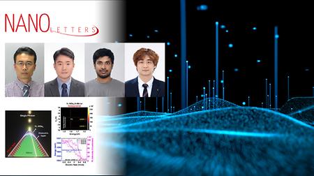
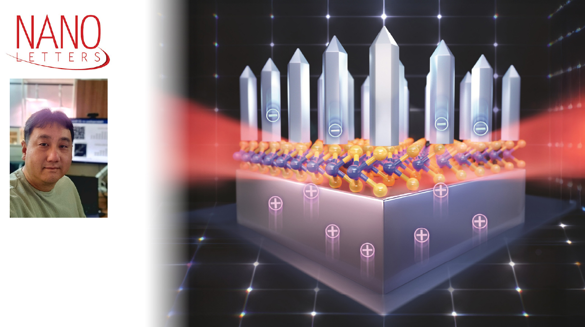
UNIST Unveils Transfer-Free Method for 2D Semiconductor LED Production
Their findings have been featured as Supplementary Cover of Nano Letters and published online on April 21, 2026.
- Research
- JooHyeon Heo
- 2026.06.04
- 958
Abstract
A research team, affiliated with UNIST has demonstrated a new way to produce light-emitting diodes (LEDs) using atomically thin layers of molybdenum disulfide (MoS2). By growing the material directly on a substrate, they eliminate the need for transferring fragile 2D films—a step that has limited previous efforts to scale and uniformity.
Led by Professor Kunook Chung from the Graduate School of Semiconductor Materials and Devices Engineering, the team developed a process to grow high-quality MoS₂ directly on gallium nitride (GaN), then add zinc oxide (ZnO) nanorods on top to form a complete p–n junction. This approach simplifies manufacturing and results in consistent, scalable devices.
MoS2, a 2D semiconductor capable of emitting visible light at just a few atomic layers, has long promised applications in quantum light sources and integrated photonics. However, traditional fabrication methods involve synthesizing the material separately and then transferring it onto a substrate, which often introduces defects, contamination, and variability.
By growing MoS2 directly on GaN, the team avoided these issues. The process begins with depositing GaN, then carefully epitaxially growing MoS2 at high temperature. The ZnO nanorods are subsequently grown vertically on the MoS₂ layer, creating a well-aligned, high-quality heterostructure.
These devices emit red light at wavelengths of 630 nm and 705 nm, confirmed through optical testing. The emission features quantum effects like spin–orbit coupling, suggesting potential for quantum photonic applications.
Professor Chung explained, “Transfer processes have limited the scalability of 2D LEDs. Our method shows that direct growth can produce uniform, high-quality devices—similar to traditional semiconductor fabrication. This opens the door to large-scale, practical 2D optoelectronics.” He further added, “Further improvements in efficiency could lead to applications such as micro-LED displays or quantum light sources, especially in the red spectrum.”
The findings of this research have been featured as the Supplementary Cover of Nano Letters on April 21, 2026. The study has been supported by the National Research Foundation of Korea (NRF), the Ministry of Science and ICT (MSIT), the Korea Institute for Advancement of Technology (KIAT), and the Ministry of Trade, Industry, and Resources (MOTIE).
Journal Reference
Imasda Rahmatulloh, Daryll JC Dalayoan, Asad Ali, et al ., “Epitaxial n-ZnO/MoS2/p-GaN Heterostructure Light-Emitting Diodes,” Nano Letters, (2026).
Related Links


-
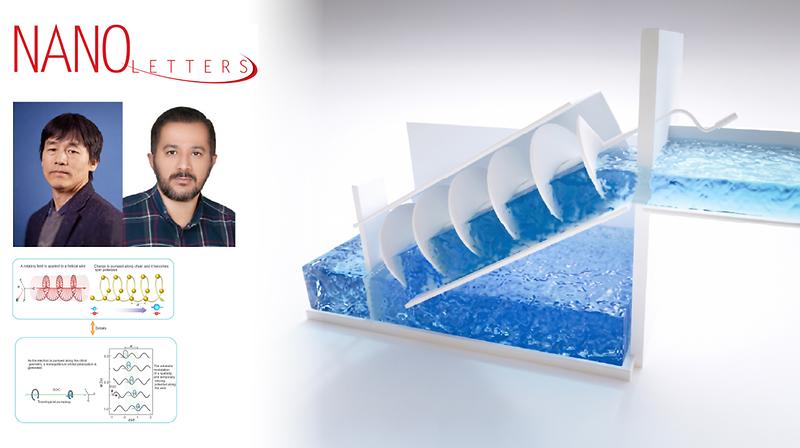
Spiral Nanowires Serve as Quantum Pumps for Quantized Electron Transport
-
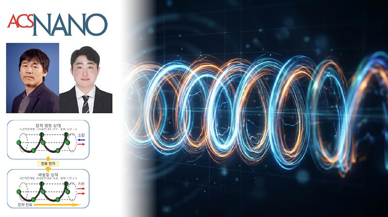
New Study Uncovers Current-Driven Spin Polarization in Chiral Nanowires
-
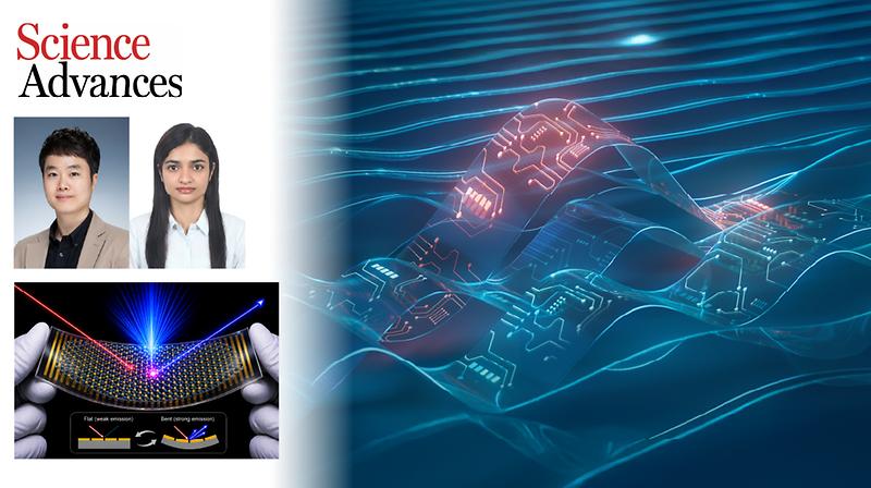
Innovative Nanoscale Design Produces Stronger Signals When Bent
-
New Study Unveils High-Purity, Electrically Controlled Single-Photon Source for Quantum Technologies